| Infrared Nano-Optics of Quantum Materials | |||
|---|---|---|---|
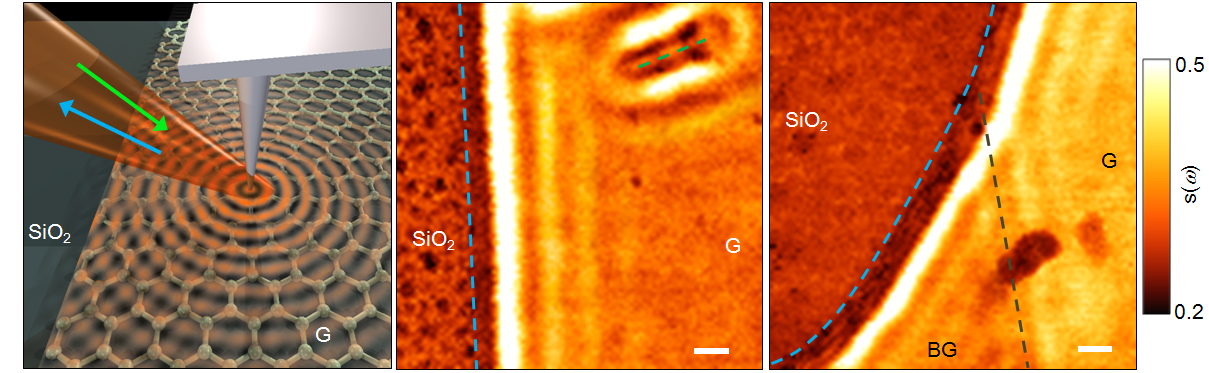
Infrared Nanoimaging of Graphene plasmons (2012)We performed infrared nano-imaging experiments of graphene on SiO2. We observed for the first time graphene plasmon fringe pattern close to the edge of graphene, defects inside graphene, even the boudary between graphene and bilayer graphene (Fig. 1). Images in Fig. 1 are consistent with the following scenario. The illuminated AFM launched plasmon waves that propagate radially away from the tip. Sample edges (or defects, boudaries) act as reflectors of the plasmon waves. When the the tip is (n/2+1/4)λp away from the edges (or defects, boudaries), the reflected plasmon waves are in phase with just launched plasmon waves, thus bright fringe form. Therefore, fringe width is exactly λp/2 , here λp is the plasmon wavelength. Thus, we are able to measure directly the plasmon wavelength from our nanoimaging results.
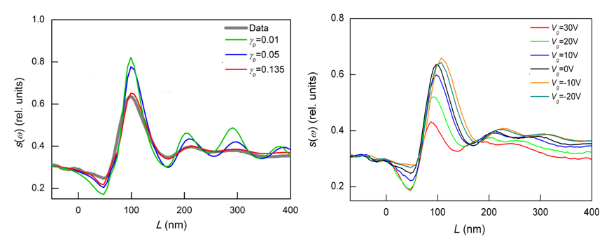
Fig. 1. Left panel: Schematics of our nanoimaging experiments. Tip launched plasmon waves interfere with themselves. Middle and Right panel: s(ω) images of graphene close to the edge revealing plasmon fringe patterns close to the edge of graphene (blue dashed lines), line defect (green dashed line), and boundary between graphene and bilayer graphene (Grey dashed line). In all paenls, G stands for graphene, BG stands for bilayer graphene, scale bar is 100 nm. In Fig. 2, we show the plasmon fringe profiles taken perpendicular to the edge of graphene. In the left panel, the grey profile is obtained from the imaging data shown above, the color profiles are our fitting results assuming various damping rates. Best fits show that the plasmon damping rate is about 0.135. In the right panel, we display the fringe profiles measured at various gate voltages, from which one can see that the plasmon fringe profiles systematically change with gate voltages indicating that graphene plasmons are truly gate tunable plasmons.
Fig. 2. Left panel: Plasmon fringe profiles taken perpendicular the edge of graphene (grey) together with our modeling results assuming various plasmon damping rates (color). Right panel: Gate tunable plasmon fringe profiles. By changing the gate voltage from 30V to -20V, graphene hole density increases monotonically due to the fact that graphene was highly hole-doped unintentionally.
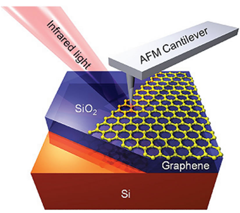
Infrared Nanoscopy of Graphene on SiO2 (2011) We performed Mid-IR nano-optic study of graphene on SiO2 (GOS). The schematics of our technique is shown in Fig. 1. Mid-IR laser is focused on the AFM tip. The strong near-field confinement of mid-IR radiation at the tip apex enable both nanoscale-resolution imaging and high-momentum probing of graphene, which cannot be achieved in conventional far-field optics. The output of experiment is near-field amplitude s(ω) and phase φ(ω).
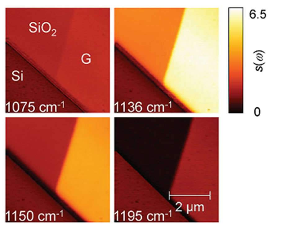
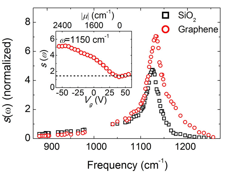
Fig. 1. Left panel: Schematics of our experimental Setup. Right panel: s(ω) images of GOS (G) and SiO2 taken at four different frequencies. s(ω) is normalized to silicon. The near-field amplitude s(ω) images about GOS were shown in the right panel of Fig. 1. These images have systematically varying s(ω) signal on both SiO2 and graphene. In the left panel of Fig. 2 we present these results in the form of s(ω) spectra. The spectra of SiO2 reveals a resonance at ω= 1128 cm-1 due to the surface optical phonon of SiO2. Graphene greatly enhances the s(ω) signal in the 1110 - 1250 cm-1 spectral region and also blue-shifts the SiO2 resonance by about 10 cm-1. Gating experiments (inset) performed at ω= 1150 cm-1 shows that the enhancement is tunable by gate voltages.
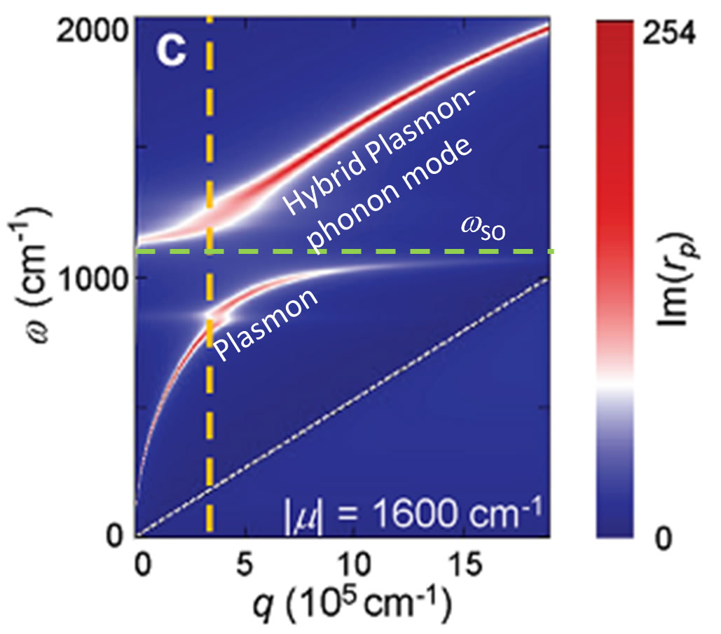
Fig. 2. Left panel: s(ω) spectra of GOS and SiO2 obtained from images in Fig. 1. The inset shows gate induced evolution of s(ω) at 1150 cm-1. Right panel: Dispersion diagram of GOS revealing plasmon-phonon coupling. Yellow dashed line marks the dominating momentum, green dashed line marks the SiO2 phonon. The enhancement and blue-shift of the phonon resonance by graphene can be understood by the dispersion diagram shown in the right panel of Fig. 2. Without graphene, the surface phonon of SiO2 appears to be a horizontal line at ωso.When graphene is on top of SiO2, the phonon mode becomes coupled with graphene plasmon mode, thus becomes a dispersive new mode (hybrid plasmon-phonon mode) that is blue shifted compared to ωso. The chemical potential of GOS is about 1600 cm-1 according to our Raman probing result. Charge dynamics in Graphene (2008, 2009)
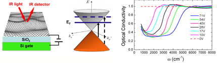
Graphene—a single layer of carbon atoms arranged in a honeycomb lattice—has very high conductivity that can be tuned by applying a gate voltage. The charge carriers in graphene can travel ballistically over great distances (~1 micron) without scattering. These unusual electronic properties make graphene a promising candidate for future nanoelectronics. The charge carriers in graphene are found to behave like relativistic Dirac quasiparticles with linear energy–momentum dispersion, which lead to a spectrum of fascinating new physics such as an anomalous quantum Hall effect and relativistic tunneling. Recently, in collaboration with E.A. Henriksen, Z. Jiang, P. Kim, H.L. Stormer (Columbia) and Z. Hao, M.C. Martin (ALS), we performed an infrared spectromicroscopy study of charge dynamics in graphene integrated in gated devices [1]. Our measurements verified that electrons in graphene behave like Dirac quasiparticles. Moreover, we discovered several unexpected results that are beyond the theoretical predictions for idealized graphene. Several observations are indicative of many-body interactions: interactions between electrons and the honeycomb lattice or mutual interactions among electrons [1].
Left panel: A schematic of the graphene sample integrated in a gate-tunable device. Infrared transmission and reflectance were measured with applied gate voltages. Middle panel: the band structure of graphene, with the Fermi energy (EF) and the absorption threshold at twice the Fermi energy (vertical lines). Right panel: The optical conductivity of graphene at different gate voltages, which is the absorption spectrum of infrared light. The threshold feature is due to the absorption onset at twice the Fermi energy. Afterwards, we performed infrared spectroscopy study of bilayer graphene integrated in the same gated structure. We found that there is a significant asymmetry in the optical conductivity upon field doping of electrons and holes, which revealed a marked asymmetry between the valence and conduction bands.[2]
Recent Publications: 4. Z. Fei, A. S. Rodin, G. O. Andreev, W. Bao, A. S. McLeod, M. Wagner, L. M. Zhang, Z. Zhao, G. Dominguez, M. Thiemens, M. M. Fogler, A. H. Castro-Neto, C. N. Lau, F. Keilmann, D. N. Basov. "Gate-tuning of graphene plasmons revealed by infrared nano-imaging". Nature (2012). 3. Z. Fei, G. O. Andreev, W. Bao, L. M. Zhang, A.S.McLeod, C. Wang, Z. Zhao, G. Dominguez, M. Thiemens, M. M. Fogler, M. Tauber, A. Castro-Neto, C. N. Lau, F. Keilmann, D. N. Basov. “Infrared Nanoscopy of Dirac Plasmons at the Graphene-SiO2 interface” Nano Lett. 11(11), 4701-4705 (2011). PDF 2. Z. Q. Li, E. A. Henriksen, Z. Jiang, Z. Hao, M. C. Martin, P. Kim, H. L. Stormer, and D. N. Basov, "Band Structure Asymmetry of Bilayer Graphene Revealed by Infrared Spectroscopy", Phys. Rev. Lett. 102, 037403 (2009).PDF 1: Z.Q. Li, E.A. Henriksen, Z. Jiang, Z. Hao, M.C. Martin, P. Kim, H.L. Stormer, and D.N. Basov, "Dirac charge dynamics in graphene by infrared spectroscopy", Nature Physics 4, 532 (2008).PDF |
|||
t |
|||