| Infrared Nano-Optics of Quantum Materials | |||
|---|---|---|---|
Molecular and organic nano-electronics
Organic electronics is currently experiencing a surge of activities worldwide prompted in part by recent advances in achieving high electronic mobility, light emission over a broad range of frequencies, demonstration of spin valve operation with giant magneto-resistance and other effects. Despite these encouraging premises, there are many roadblocks that hinder a broader proliferation of plastic electronics in contemporary technology. Arguably, the most significant of them is the challenge to achieve a comprehensive understanding of the fundamentals of charge injection and charge transport in polymers. Recently, in collaboration with A.J. Heeger (UCSB), Vitaly Podzorov and Michael Gershenson (Rutgers), we have investigated charge injection effect in the field effect transistor (FET) based on organic molecular crystals [1] and polymers [2]. Combined with IR microscopy these new experimental capabilities promise to deliver a comprehensive understanding of energy, length and time scales involved in the injection processes in the FET structures. This work is currently supported using funding from the NSF Organics program and from the Petroleum Research fund for this research area. (a): Molecular crystal FET's
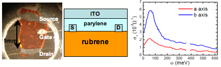
Left panel: A photograph of a FET device based on single crystal rubrene. Middle panel: A schematic of the device structure of rubrene FETs. Right panel: the optical conductivity of the accumulation layer in rubrene FETs at a gate voltage of -280V at 300K, with the E vector of the IR light along the a and b axis of rubrene. Our data indicate that transport in rubrene is governed by light quasiparticles in molecular orbital bands, and the polaronic effects in rubrene FETs are weaker at room temperature than previously thought [1]. (b): Donor-Acceptor (DA) conjugated polymer FETs
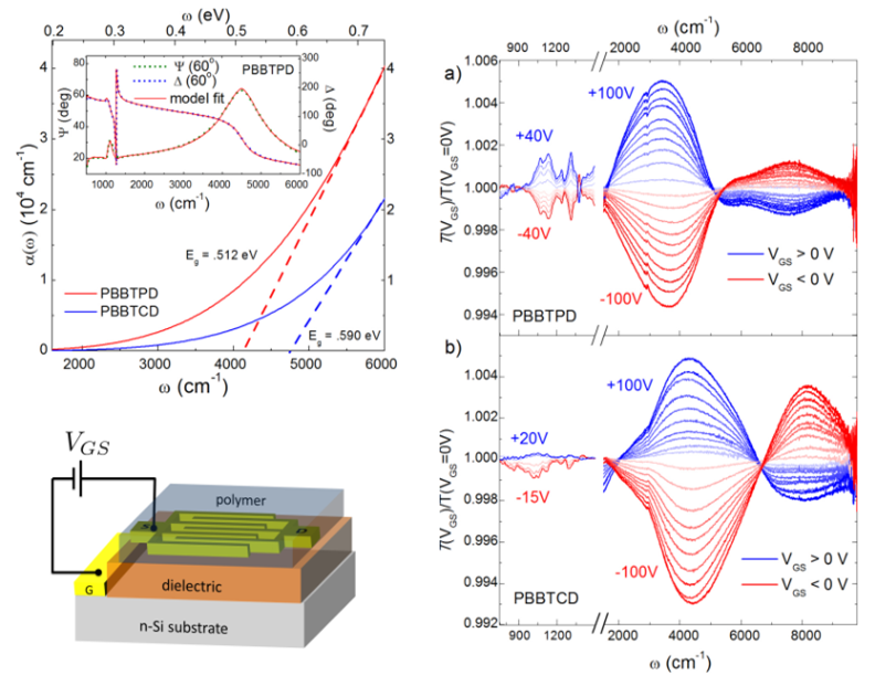
There is considerable interest in ambipolar polymers for use in organic complementary logic electronics similar to standard Silicon CMOS technology. One very efficient way to achieve intrinsic ambipolarity in conjugated polymers is through the use of donor-acceptor (DA) structures. In addition to ambipolarity, the inherent tunability of the band gap with appropriate donor and acceptor moeities highlights DA systems as very useful materials for photovoltaic and light-emitting devices as well. We carried out a thorough infrared study of ambipolar charge injection in narrow-gap DA polymer transistors. The top left panel shows a detailed characterization of the absorption edge for DA polymers based on benzobisthiadiazole (BBT), exhibiting extremely small band gaps below 1 eV. Employing infrared spectroscopy, we have been able to directly probe the electronic excitations associated with injecting both electrons and holes in a functional organic FET device, shown on the lower left. This work is the first of its kind. Right panel: voltage-induced change in IR transmission for OFET devices based on (a) PBBTPD and (b) PBBTCD. We observe IR-active vibrational modes (sharp resonances in 800-1300 cm-1 region) as well as a significant modification of the polymer absorption edge in response to the applied electric field. The absorption edge reveals hardening under electron injection and softening under hole injection. These findings indicate that several physical processes likely contribute to the field-induced changes in IR transmission spectra. These processes include: electron- and hole-induced polaron absorption, and/or electric field-induced modulation of the polymer band edge (the linear Stark effect). The latter effect implies the existence of a significant electrical dipole moment in these DA polymers. Recent Publications: 1. O. Khatib, J. D. Yuen, J. Wilson, R. Kumar, M. Di Ventra, A. J. Heeger, D. N Basov. "Infrared spectroscopy of narrow gap donor-acceptor polymer-based ambipolar transistors" Phy. Rev. B 86, 195109 (2012). 2. O. Khatib, B. Lee, J. D. Yuen, Z. Q. Li, M. Di Ventra, A. J. Heeger, V. Podzorov, D. N. Basov,"Infrared signatures of high carrier densities induced in semiconducting poly(3-hexylthiophene) by fluorinated organosilane molecules", J. Appl. Phys. 107, 123702 (2010). 3. Z. Q. Li, V. Podzorov, N. Sai, M.C. Martin, M.E. Gershenson, M. Di Ventra and D.N. Basov, “Light Quasiparticles Dominate Electronic Transport in Molecular Crystal Field-Effect Transistors”, Phys. Rev. Lett. 99, 016403 (2007). 4. Z. Q. Li, G. M. Wang, N. Sai, D. Moses, M. C. Martin, M. Di Ventra, A. J. Heeger, and D. N. Basov, “Infrared Imaging of the Nanometer-Thick Accumulation Layer in Organic Field-Effect Transistors”, Nano Letters 6 (2), 224 (2006). 5. Z.Q. Li, G.M. Wang, K.J. Mikolaitis, D.Moses, A. J. Heeger, and D.N. Basov, “An infrared probe of tunable dielectrics in metal-oxide-semiconductor structures”, Appl. Phys. Lett 86, 223506 (2005). |
|||
t |
|||